The beauty of programmable logic devices (PLDs/FPGAs) and why they matter today
A brief introduction into modern programmable logic devices (PLDs), like FPGAs from the manufacture Intel (formerly Altera) and why it could be interesting to work with them.
A brief introduction into modern programmable logic devices (PLDs), like FPGAs from the manufacture Intel (formerly Altera) and why it could be interesting to work with them.
Welcome to the first rsyocto Blog Post! With this blog I will reveal the beauty of modern SoC FPGAs, show their advantages in the embedded market and give an overview of complex embedded SoC FPGA design with practical examples for the next generation of applications.
Motivation for taking FPGAs in mind for the next generation application design
The global chip shortage, which has slowed production since 2021, has shown that the urge for non-food consumer goods is much greater than the few semiconductor manufacturers can satisfy. They must produce an endless number of different application specific integrated circuits(ASICs) containing hard-wired logic. On the other hand, Field-Programmable Gate Arrays (FPGAs), are also be produced in semiconductor fabs, but they can load an endless number of wired logics by just loading the configuration. This unique capability of FPGAs enables the semiconductor industry to build always the same device for a ton of applications in a high volume. The crises show me that the demand for high-performance intelligent devices is higher since ever before.
Artificial intelligence (AI) is one of the biggest trends of the decade and the underlying know-how as seen as the most important technology of the 21st century. IDC (International Data Corporation) Insiders expect a global spending of $110 billion in this market in 2024. This is three times as much as in 2019. They predict an explosion of the machine learning market in the next years [1].
AI capable products will be used in a hole variety of areas, such as consumer products and connected industrial internet of things (IIoT). They can help answering scientific questions, putting a self-driving car on the road, or improving cybersecurity. While the first robots in the workplace were mainly involved with automating manual tasks such as manufacturing and production lines, today's software-based robots will take on the repetitive but necessary work that we carry out on AI controlled computers [2]. It is widely accepted that whoever controls the strongest artificial intelligences controls the world [3].
Deep learning, as a part of AI, is a computer software that mimics the network of neurons in a brain. Today cloud service providers like AWS (Amazon web services), Microsoft Azure and IBM are the biggest drivers in this market. They want to offer new AI services to their customers to allow to improve their workflows. They will connect millions of devices with cloud datacentres to process the accruing data centralist.
To achieve the full potentials of AI applications by keeping power consumption moderate special optimized AI accelerator units are required, which are connected to CPUs. Typical CPU instruction sets are not designed for these tasks and often too inefficient. Therefore, GPUs (Graphics Processing Units) are in use today. The leading GPU manufacture NVIDIA offers PCIe (Peripheral Component Interconnect Express) GPU accelerator cards for cloud data center providers. NVIDA’s CUDA framework is able to execute source code with a high parallelization on thousands of CUDA Cores inside their GPUs.
On the other hand, modern high-end FPGAs, for instance the Intel Arria 10 family, contain sometimes millions of small logic elements (LEs), which can completely operate independent to each other to bring the highest parallel processing performance of any other technology to the table. They can execute complex mathematical or digital signals processing (DSP) calculations in a single clock cycle. CPUs and GPUs would need thousands of steps to find the same result. For instance, a while ago, as a FPGA newcomer, I designed a prime number generator with an Intel Cyclone V FPGA board, that could find large prime numbers faster than any other device with such a low power consumption.
The disadvantage and certainly the main reason why FPGAs are by far not as populated as GPUs is the complexity of the required Hardware Description Language- (HDL) and software development to realise a simple project. NVIDA’s CUDA software framework enjoys a wildly integration in almost every major accelerator environment, like for example Google TensorFlow, to enable a smooth GPU acceleration out of the box. Unfortunately, this is not the case for FPGA-based accelerators. To counteract this issue, Intel, for example, developed the OpenVino toolkit and the OneAPI to allow the acceleration of typical AI models with FPGAs for a cloud environment. Intel benchmarks its FPGA concept in comparison with CPU- and GPU solutions. Intel demonstrates with typical deep learning models as reference that FPGA accelerators can process AI applications up to 19.9 times faster than typical CPUs [4]. It has therefore been proven that special optimized accelerators are required for AI applications and FPGAs have suitable potentials for such tasks.
A research project conducted by Microsoft on an AI Image classification task shows that Intel Arria 10 FPGAs have, beside their higher raw performance, an almost ten times better power consumption than compatible GPUs [5]. For cloud providers the power consumption and the cooling of typical thousands power-hungry servers are one of the biggest issues. It can be assumed that with the growth of the AI market and the number of connected devices, the power consumption in data centers will increase significantly. The enormous amount of energy and heat waste, datacenters will consume, cannot be viewed as an environmentally friendly goal for the future.
Beside the acceleration of deep learning tasks, FPGA accelerator cards can be used for hundreds of different applications, as well. For example, they can help to increase rapidly the performance of Image processing, encryption methods and compression algorithms. Accelerator cards use the same bus interface called PCI Express (PCIe) to interact with the Host CPU running a hypervisor to share the acceleration performance. In this market they compete with special designed Data Processing Units (DPUs), another big industry trend, like the NVIDIA (Mellanox) BlueField DPU family.
Further, it is predictable that industrial and automotive companies will need independent local accelerator solutions to enable more efficient manufacturing. A permanent online high-speed cloud connection is often not suitable for them. Typical industrial and automotive AI applications, such as object detection for waste sorting in a recycling line, are safety critical. They must comply with strict rules. Often employees must work in the nearfield and fail-safety is an important factor. Additionally, for controlling an actuator with real-time commands a high-speed low latency connection is necessary. These requirements with cloud solutions today are not reachable by far, because the required high-speed fiber optic network infrastructure in most regions is not available or the link latency is too instable.
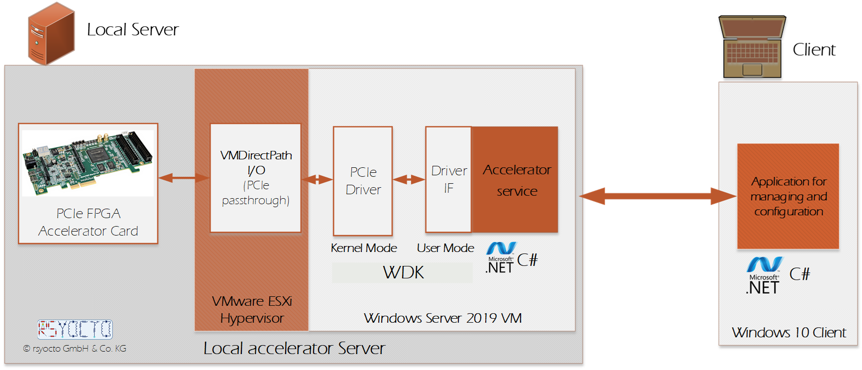
For a research project in 2019 I took a typical cloud-based accelerator approach to a local server assigned to the local scientifical platform. The accelerator environment consists of a Windows Server 2019 virtual machine running on a VMware ESXi Hypervisor and an attached Intel PCIe FPGA accelerator card. The virtualization approach allows a fail-safety operation and maintenance during runtime and is standard in the public cloud. For the realization it was necessary for me to configure a VMware ESXi Host with enabled PCIe Passthrough. The server was placed in a server room in the nearfield to allow a low latency fiber optical connection to actuators and sensors. This is by far not reachable with typical Cloud-, GPU- or FPGA solutions. To successfully implement this project, it was necessary for me to design the entire acceleration flow from scratch. I developed a Windows Kernel mode driver with Microsoft’s official driver development kit (WDK) to get the full capabilities of the Windows operating system. The driver supports up to eight PCIe accelerator cards, which are combined in a cluster, as well as every Intel FPGA PCIe device with different PCIe generations. Every driver developed with the WDK requires a specially developed Windows user mode interface. It was developed to enable integration as a Dynamic Link Library (DLL) at a high-level C# application. This application runs in the background of the virtual machine as a service and can contain the CPU part of the acceleration task. A Windows 10 computer connected over a HTTP connection to the accelerator server can present a graphical user interface (GUI) for interacting with the acceleration environment. To achieve that, I used Windows communication framework (WCF) and the Windows presentation foundation (WPF).
My designed accelerator environment could help to design specific industrial and automotive accelerator applications during the research phase. With the high degree of integration and combination of the FPGA- and the desktop world, this project can show how powerful and future-oriented both sides can work together and reveals with this example the potential of FPGAs.
For edge computing SoC (System on Chip) FPGAs are a great choice. SoC FPGAs are combining a FPGA Fabric, that can be solved as an accelerator unit and an Arm Hard Processor System (HPS), for running an Embedded Linux Distribution. Additionally, the FPGA Fabric can implement complex sensor interfaces for instance cameras, LIDAR or Radar. The FPGA-Portion can implement any special legacy interfaces or run safety critical tasks completely in hardware, as it is usually required for embedded long-term projects. This can help to simplify the overall system complexity and to decrease the length of the low latency Datapath between processing system and the accelerator. On the other hand, a highly optimized Embedded Linux Distribution for executing commonly used deep learning tasks can be considered to connect for instance with the modern cloud- and desktop-world. This high-level flexibility in a single package is a unique selling point for SoC FPGAs. However, the development effort of these SoC-FPGA accelerator platforms will be rapidly increase. To counteract this effect powerful complex development tools become more and more important.
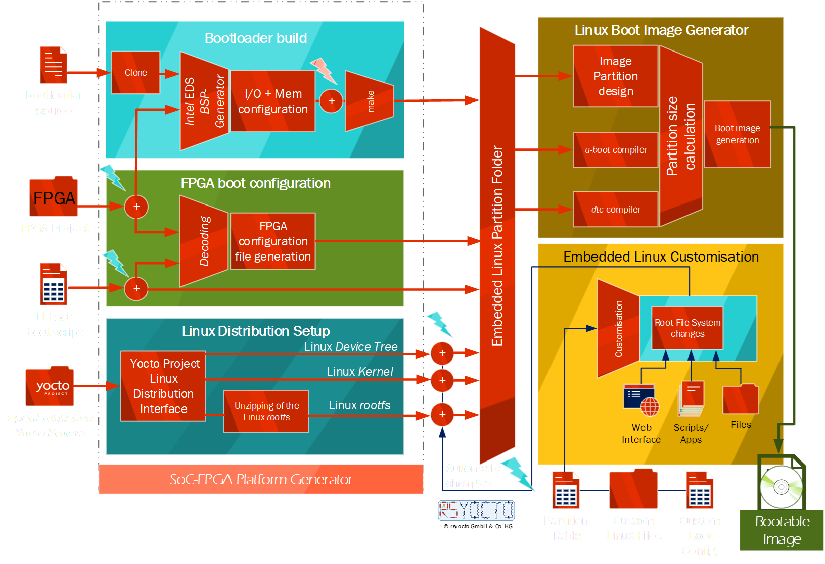
For that reason, I designed for Intel SoC FPGAs an optimized Embedded Linux Distribution with the OpenEmbedded Yocto Projectwith a highly integrated build system to simplify the complex and time-consuming development effort required for modern SoC FPGA designs. This concept allows a high-level Application specific Optimization for embedded solutions in a simple fashion as it cannot achieve with any other approach. It enables, for instance, to build automatically a Linux Distribution accelerating FPGA Soft-IP components with specific Linux Kernel Mode Drivers.
Intel FPGAs as programmable logic devices (PLDs)
Programmable logic devices (PLDs) are integrated semiconductors, which can load almost every digital circuit in seconds. They were invented in the 1980s to bring free configurable clue logic into a chip. At this time no one could imagine, that today’s programmable devices can implement complex digital systems, such as Microprocessors. In the earlier days, PLDs could only be considered for simple interface applications. However, at the first time in the semiconductor history it was not necessary to design and manufacture application specific integrated circuits (ASICs) for such tasks. This increases the time to market and reduces the manufacturing cost rapidly. With the Moor’s law driven decreasing CMOS transistor size it is possible to fit more and more circuities inside a chip. After every manufacturing size decreasement PLDs can take an advantage of even more than it is possible with CPUs. Because then they can handle more logic and do not require complex software changes, which are necessary by the typical increasing core count of CPUs today. The revolution of the programmable logic devices (PLDs) had started with the Complex Programmable Logic Devices (CLPs) which store their logic circuit in non–volatile EEPROM cells. Modern concepts of PLDs use SDRAM based cells for configuration their logical circuity. They are known as Field Programmable Gate Arrays (FPGAs). This improves the performance and simplifies the chip design. That allows semiconductor manufactures to implement a higher count of logic inside a single chip. However, a disadvantage is, that FPGAs cannot hold their configuration during a power-off state, as it is possible with EEPROM based CLPs.
Modern FPGAs consist of mixes of configurable static random-access memory (SRAM), high-speed input/output pins (I/Os), logic blocks, and routing. These logic blocks are naturally called logic elements (LEs). One unit can be connected in rows and columns together with others to implement any kind of logic. For example, one LE can build a logic NOR-gate. They can also be connected to memory cells, too. This SRAM allows to design logic with high-speed memory embedded. Typical FPGAs have a huge count of In- and Out-Pins (I/Os) to interact with their outer world. For example, a high count of data lanes is required for the connecting of high-speed parallel interfaces, such as a camera or external SDRAM modules. In addition to the general purpose in- and outputs (GPIOs) pins are often special independently useable transceivers embedded, as well. They allow a high-speed data transfer and they are often used for example to connect PCIe lanes or fiber optical InfiniBand network interfaces to the FPGA. With these high flexibility FPGAs are perfect candidates for highly optimized wired- and wireless network applications, such as network switches or satellite communication. Based on the fact that FPGAs can implement the behavior of environment changes in hardware they can be considered for safety critical low latency applications. Only ASICs can compete in this area with FPGAs. General microcontrollers have to calculate their reaction with the software and this always takes some clock cycles.
Intel acquired Altera, beside Xilinx and Microsemi, a well-known manufacture of programmable logic devices in 2015. For combining the benefits of CLPs with FPGAs Intel had announced the Intel MAX 10 FPGA family. MAX 10 devices do not only include a full featured FPGA Fabric but they also embedded up to two flash memories and an Analog-to-Digital Converter (ADC). This brings the capability of instant power ON devices to the market. With integration of Low-Dropout Regulators (LDOs) they did not require a complex PCB circuity with different power rails, as typical FPGAs are known for. That makes MAX 10 FPGA devices the perfect candidates of replacing hardware related microcontroller solutions with them.
Intel offers for their entire FPGA family a soft-core processor called NIOS II. This 32-Bit microcontroller is highly customizable and can be loaded to the FPGA Fabric. Recently, they announced their RISC-V based implementation, named NIOS V for their heigh-end FPGA devices as soft-core processor for running an embedded real-time OS (RTOS). Even, a soft-core RISC-V application processor, that runs complex Linux shall come soon.
The main difference to Intel’s Cyclone 10 LP family is that they have none FLASH storage implemented and for that reason they require an external configuration device. This increases the necessary Bill of Materials (BOM) and the required effort for securing the FPGA configuration process. Additionally, Intel Cyclone 10 GX FPGAs 12.5 Gbps transceivers, a Hard IP SDRAM- and PCIe- interfaces are embedded. This makes them perfect for industrial or automotive embedded vision camera systems to mention only a few applications. With the Cyclone 10 generation Intel could decrease the cost and the power consumption of these devices. Today the Intel Cyclone V SoC FPGAs from the last generation are not refreshed. SoC FPGAs combine the FPGA Fabric with an Arm based Hard Processor System (HPS). On these ARM CPU cores it is possible to execute for instance Desktop image processing software. Then the FPGA can implement a camera sensor interface with some image pre-processing and filtering. With the highly optimized internal Arm AXI interfaces and shared-memory interfaces between the FPGA and the HPS image processing with lower frame lacks are possible. Beside the use of the Cyclone V SoC-FPGAs as a system on chip (SoC) for image processing applications it can also be considered for any desktop related acceleration tasks. For high- end applications the Intel Arria 10-, Intel Stratix 10- and Agilix family of FPGAs are available. Intel Arria 10 FPGAs offer a high count of logic elements in the million region and they implement transceivers up to 28.3 Gbps. With the integration of secure FPGA configuration managers, they are designed for high-end safety critical applications. With the Intel Arria 10 SX is a SoC-FPGA class with ARMv7a Cortex A9 Dual-Core HPS available. For the Intel Stratix 10- and the previously announced Intel Agilix FPGAs are an ARMv8a 64-bit Cortex A-53 on stock. The Intel Agilix FPGAs are primary only as a SoC FPGA version available and bring various of different chiplets with for instance ultra-high-speed up to 224Gbit Ethernet, PCIe Gen5 with CXL (Compute Express Link) and on-chip HBM (High Bandwidth Memory) memory to enable advanced high-end application in future.
Especially, the high-end FPGA devices can show the endless capabilities, flexibility and use cases for modern FPGAs that can not be achieved with any other technology on the market.
rsyocto is an embedded SoC FPGA services provider to takes over and automate the complex SoC FPGA development so that its partners can focus on their big thing by getting their applications accelerated with ground-breaking SoC FPGAs.